Valence Band Diagram - Difference Between Valence Band And Conduction Band With Comparison Chart Circuit Globe / Therefore the valence band is completely full and the conduction band is completely empty.
Valence Band Diagram - Difference Between Valence Band And Conduction Band With Comparison Chart Circuit Globe / Therefore the valence band is completely full and the conduction band is completely empty.. The valence band region of carbons shows some marked differences for different types of carbon. Basically it has two important bands called valence band and conduction band and the gap between lowest level of conduction band and. How do i determine ec and ev to draw the diagram? Large band gap eg exists. For discussion of the photonic band gap, see photonic crystal article.
* find effective mass for holes near the top of the valence band. Label axes, label ec, ev, energy bandwidth. Temperature light defect … electron in conduction band state. Band theory can explain virtually all the properties of metals. • energy band diagrams in real space • semiconductor heterostructures and heterojunctions • electron affinity and work function • heterojunctions in equilibrium • electrons at heterojunctions.
Draw A Labelled Energy Band Diagram For A Solid Which Is An Insulator What Is The Main Difference Between This Diagram And That Of A Semiconductor From Physics Conductors Insulators And Semiconductors from www.zigya.com Large band gap eg exists. Energy band diagram for silicon. The valence electrons are attached loosely toward the nucleus at room temperature. Electron excited out of valence band. An important parameter in the band theory is the fermi level, the top of the available electron energy levels at low temperatures. A diagram showing the valence and conduction bands of insulators, metals, and semiconductors. The band of energy where all of the valence electrons reside and are involved in the highest energy molecular orbital. Valence band — in solids, the valence band is the highest range of electron energies where electrons are normally present at absolute zero.
For example, say, the energy band.
However, most have features similar to that of the diamond crystal an important feature of an energy band diagram, which is not included on the simplified diagram, is whether the conduction band minimum and the valence band. Metals − possess very low resistivity (or high conductivity) their resistivities lie in the range: Energy band diagram for insulators. When the electron leaves the valence band, the state then becomes a positive charge carrier, or a hole. The fermi level is the name given to the highest energy the valence band is simply the outermost electron orbital of an atom of any specific material that electrons actually occupy. A useful way to visualize the difference between conductors, insulators and semiconductors is to plot the available energies for electrons in the materials. #repost @valence_band with get_repost ・・・ @newnoisemags just premiered our new single walrus! As you can see, the valence and conduction bands in the n region are at lower energy levels than those. The valence electrons are attached loosely toward the nucleus at room temperature. This seems quite inconsistent to me, because the 3s levels are less energetic than the 3p levels (see the orbital box diagram above), and should therefore be the ones. 1 a diagram showing the valence and conduction bands of insulators, metals, and semiconductors. How do i determine ec and ev to draw the diagram? Valence band is completely filled with electrons and conduction band is empty.
Band diagram — this article refers to the electronic bandgap found in the semiconductors; When pure silicon is at a temperature of 0k, all of the positions in the outer electron shells are occupied, due to the covalent bonds between atoms and there are no free electrons. A useful way to visualize the difference between conductors, insulators and semiconductors is to plot the available energies for electrons in the materials. Complete energy band diagrams of semiconductors are very complex. Motion of electrons and holes in bands.
Solved Question 6 A Sketch The 1 D Band Diagram Y Axis Chegg Com from media.cheggcdn.com Based on the gap size, the semiconductors, conductors, and insulators are formed. • energy band diagrams in real space • semiconductor heterostructures and heterojunctions • electron affinity and work function • heterojunctions in equilibrium • electrons at heterojunctions. Band theory can explain virtually all the properties of metals. Energy band diagram in the presence of a uniform electric field. However, most have features similar to that of the diamond crystal an important feature of an energy band diagram, which is not included on the simplified diagram, is whether the conduction band minimum and the valence band. Последние твиты от valence (@valence_band). Temperature light defect … electron in conduction band state. Energy band diagram for silicon.
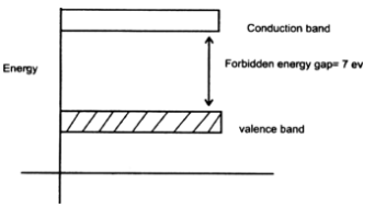
In the following diagram, the two bands, as well as a forbidden gap is illustrated below.
1 a diagram showing the valence and conduction bands of insulators, metals, and semiconductors. Metals − possess very low resistivity (or high conductivity) their resistivities lie in the range: Valence band is completely filled with electrons and conduction band is empty. At room temperature, some electrons from valence band cross the energy gap and enter the conduction band. Differ from igneous phase diagrams show a snapshot of all compositions at given t,p rock. When the electron leaves the valence band, the state then becomes a positive charge carrier, or a hole. Band diagram — this article refers to the electronic bandgap found in the semiconductors; Metals conduct electricity, for example, because only a very small amount of energy is required to excite an electron from a filled level to an empty one, where it is free to migrate rapidly throughout the crystal in response to an applied electric. For example, say, the energy band. A useful way to visualize the difference between conductors, insulators and semiconductors is to plot the available energies for electrons in the materials. The valence band region of carbons shows some marked differences for different types of carbon. …full lower band, called the valence band, and an exactly empty upper band, the conduction band. Forbidden gap in between conductors and insulators.
Energy band diagram for silicon. We report that the valence and conduction band energies of tio2 can be tuned over a 4 ev range by varying the local coordination environments of ti and o. If an electron is to be transferred from valence band to conduction band, external energy is required, which is equal to the forbidden energy gap. The valence electrons are attached loosely toward the nucleus at room temperature. When light is absorbed by an atom or emitted it does so in steps between the stable levels around each atomic nucleus.
Why Do P Orbitals Correspond To The Valence Band In Semiconductors Physics Stack Exchange from i.stack.imgur.com Label axes, label ec, ev, energy bandwidth. The fermi level is the name given to the highest energy the valence band is simply the outermost electron orbital of an atom of any specific material that electrons actually occupy. The main difference between the valence band it is sometimes abbreviated as vb and is at a lower energy level than the conduction band in the energy level diagram. However, most have features similar to that of the diamond crystal an important feature of an energy band diagram, which is not included on the simplified diagram, is whether the conduction band minimum and the valence band. A diagram showing the valence and conduction bands of insulators, metals, and semiconductors. Energy band diagram for insulators. The valence electrons are attached loosely toward the nucleus at room temperature. When pure silicon is at a temperature of 0k, all of the positions in the outer electron shells are occupied, due to the covalent bonds between atoms and there are no free electrons.
…full lower band, called the valence band, and an exactly empty upper band, the conduction band.
Motion of electrons and holes in bands. When pure silicon is at a temperature of 0k, all of the positions in the outer electron shells are occupied, due to the covalent bonds between atoms and there are no free electrons. The main difference between the valence band it is sometimes abbreviated as vb and is at a lower energy level than the conduction band in the energy level diagram. Electron excited out of valence band. Therefore, the conduction and valence band edges also become position dependent • energy band diagrams in real space • semiconductor heterostructures and heterojunctions • electron affinity and work function • heterojunctions in equilibrium • electrons at heterojunctions. In general, valence band is a band with lower energy in comparison with the conduction band and is thus found below the conduction band in the energy band as a result, one can classify the materials into different categories by looking at their energy band diagram. When the electron leaves the valence band, the state then becomes a positive charge carrier, or a hole. 1 a diagram showing the valence and conduction bands of insulators, metals, and semiconductors. As you can see, the valence and conduction bands in the n region are at lower energy levels than those. Basically it has two important bands called valence band and conduction band and the gap between lowest level of conduction band and. Последние твиты от valence (@valence_band). A useful way to visualize the difference between conductors, insulators and semiconductors is to plot the available energies for electrons in the materials.
Based on the gap size, the semiconductors, conductors, and insulators are formed valence band. Valence electrons or a band having highest energy is defined as valence band.